The main driving force behind the rapid growth in digital technology has been scaling the transistors to extremely small dimensions. This reduction of dimensions has resulted in the possibility of packing more transistors in a given area leading to an increase in the computing power as well as functionality of electronic devices. Smaller dimensions also lead to a smaller capacitance of the devices which helps in increasing the frequency of operation of transistors. However, the minimum supply voltage possible for transistors has been limited by the fundamental Boltzmann limit, according to which, when carriers are injected into the channel from the source through thermionic injection, the subthreshold slope cannot be less than 60 mV/decade at room temperature. This inability to scale supply voltage has led to a rapid increase in the power consumption of transistors.
TFET offers an interesting solution to this problem1 by exploiting band-to-band tunnelling of carriers rather than thermionic emission. Promising TFET transistors have been shown previously with both homojunction (Silicon and Germanium) and heterojunction (III-V semiconductors)2. However, the difficulties in obtaining good material interfaces, a sharp doping profile, and efficient gate control are the main challenges in this direction. Layered vdW materials can potentially overcome these problems since the formation of heterojunction with layered materials is not constrained by the lattice matching of the successive layers3, providing an atomically sharp and ultra-clean interface. In addition, due to the atomically thin nature of the layers, it is possible to tune the interface effectively using gate voltage.
Band-to-band tunnelling has been explored in several vdW heterojunctions including /4, BP/5, BP/6, Ge/7 and /8–12 heterojunctions. Among these systems, /heterojunction has led to considerable interest8–13 due to a broken gap (type-III) band alignment in such a system. Broken gap heterojunction relaxes the requirement for a large external electric field to achieve a large band-to-band tunnelling current density.
Self-alignment between the channel and the source/drain regions plays a crucial role in MOSFET technology. This is achieved during the fabrication process by cleverly sequencing the gate stack fabrication and the source/drain doping. However, the lack of a conventional doping process (such as ion implantation) hinders such self-alignment in devices with layer materials. Instead, a majority of such layer material-based field-effect devices depend on gate-induced electrostatic doping in the contact region, often confounding the intrinsic device operation. It will be thus useful to have a test structure where the performance of self-aligned devices can be easily tested.
Here we report a triple-gated / heterojunction device test structure where we achieve the source-channel self-alignment by using two partially overlapping top gates. The mode of operation can be electrostatically tuned from an n-MOSFET to a p-TFET, with the latter mode providing a sub-60 mV/decade subthreshold slope. The extraction of the intrinsic electrical characteristics of such heterojunction is often confounded by the contact series resistance offered by the metal junction. We get rid of such parasitic effects by the use of this unique gate-defined self-aligned structure.
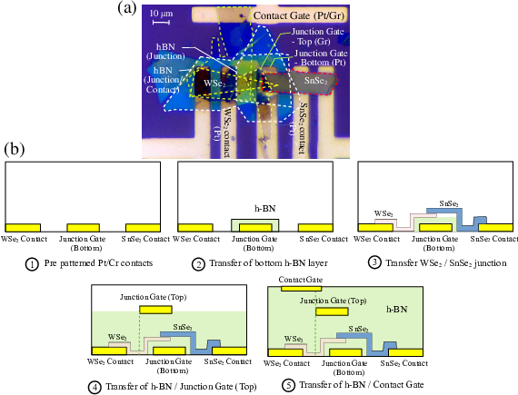
An optical micrograph of the fabricated device is shown in Figure 1.1(a). During the fabrication, pre-patterned Pt metal contacts have been created on Si/SiO\(_2\) substrate using photolithography followed by metal deposition and subsequent lift-off. All the layered materials are transferred to the pre-patterned substrate using a dry transfer method14. First, an h-BN (15-20 nm thick) layer is transferred to the top of the back gate electrode. A (3-4 nm thick) flake is then transferred on top of the bottom gate with electrical contacts being made of \(\sim\)40 nm thick Pt metal pad. Next, a \(\sim\)50 nm thick flake is transferred on top of this flake.
The back gate electrode controls the junction region of the structure. A top gate stack is then formed right on top of the / heterojunction by transferring h-BN and few-layer graphene flakes. The step-by-step transfer and fabrication flow of the device is depicted in Figure 1.1(b). The cross-section image of the final step of the process represents the cross-section of the device. The top gate is electrically shorted with the back gate for a dual-gate structure. Finally, another gate stack comprising of h-BN and few-layer graphene is transferred, which covers the heterojunction and the /Pt contact junction. The crystal used in this work is of 2H poly-type as suggested by the Raman spectrum (). The flake degenerately n-doped15 adds negligibly to the series resistance of the device.
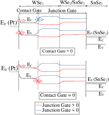
We denote the shorted top and bottom gate electrodes as the junction gate since they effectively control the junction region and the region near the junction of the device. This gate does not control the contact regions of the device. On the other hand, we label the third gate on top as the contact gate. This gate has a partial overlap with the top junction gate (see Figure 1.1(b) and is thus effectively isolated from controlling the properties of the heterojunction due to electrostatic screening of the top junction gate. Hence, this gate only controls the /Pt contact region. This way, the combination of the two top gates creates the self-aligned structure, with the two independent gates controlling the contact and junction region, as delineated by the dashed line in Figure 1.1(b). In particular, the dual-gate structured junction gate electrodes efficiently control the / junction. In contrast, the contact gate on top only controls the /metal contact region of the device.
The electrical characterization is performed at different temperatures under vacuum (\(5\times10^{-5}\) mbar pressure) in Lakeshore CRX-6.5K probe station using a Keithley 4200 parametric analyzer. As a control, we first characterize the channel with Pt contacts on both sides and use the contact gate as a top gate. The corresponding transfer characteristics exhibit strong ambipolar nature (), as is usually observed in typical channel-based field-effect devices8,16,17.
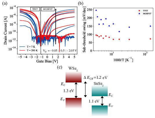
Next, we turn our attention to the heterojunction device. First, we characterize a single gated / device. By applying a suitable combination of biasing configurations, we tune the mode of operation of the device from p-TFET to n-MOSFET. Typical temperature-dependent characteristics of the / heterojunction are shown in Figure 1.2(a) measured at 7 K (blue trace) and 295 K (red trace). We observe that in the p-TFET mode (\(V_{G}<0\)), the subthreshold slope is weakly dependent on temperature. On the other hand, in the n-MOSFET mode (\(V_{G}>0\)), the carrier injection is governed by the thermal process, and the subthreshold slope depends strongly on temperature. The same is reflected in Figure 1.2(b) where sub-threshold swing is plotted as a function of \(1000/T\).
devices usually display ambipolar characteristics, which is attributed to Fermi level pinning near the middle of the band gap18. This usually results in larger contact resistance. It has been shown previously that a double gate structure can be used to mitigate this problem, where one of the gates could be used to create an efficient tunnel barrier near the contacts while the other could be used to modulate the channel properties19. This, however, usually leads to interference between the two gates; the most noticeable effect of such a structure is the shifting of the threshold voltage. In order to overcome this, we design a double gate structure near the channel, where the electrostatic screening prevents interference between the contact gate and the junction gate. The region under the contact gate in the WSe\(_2\) channel can hence be switched between p-type and n-type modes of operation without any electrical interference with the junction region. We use the p-type electrostatic doping for TFET operation and the n-type doping for regular MOSFET operation.
Next, we describe the characteristics of the proposed device. In each mode of operation described below, the contact gate is held at a fixed bias, while the junction gate is swept through the required voltage range, both in forward and reverse direction. We observe negligible hysteresis in the characteristics indicating the excellent quality of the interfaces of the graphene/h-BN/WSe\(_2\) gate stack.
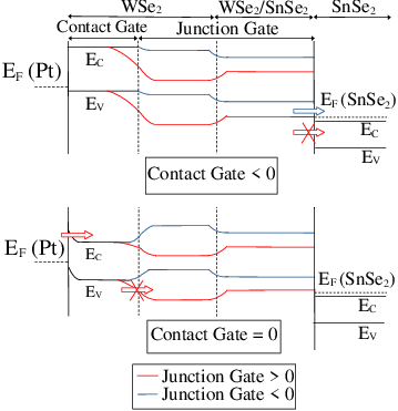
. The band diagrams and the transfer characteristics of the p-TFET are shown in Figures 1.3 and 1.4(a), respectively. In this mode of operation, we keep the electrode contacting as grounded while applying a negative bias to contact. The junction gate is then swept from \(-5\) V to \(+5\) V, while keeping the contact gate electrode biased at various negative voltages. Note that, the junction gate modulates both the regions in the / interface as well as adjacent to the interface, as shown by the band diagram in the top panel of Figure 1.3. In particular, the modulation of the bands in in the junction region is performed only by the bottom gate as the gate field from the top gate is screened by the heavily doped layer20. However, the adjacent to the junction is efficiently modulated by both top and bottom junction gates. With a more negative junction gate bias, the tunnelling window for electrons to tunnel from the valence band of to the conduction band of increases, in turn increasing the drain current (indicated by the blue arrow). On the other hand, at a more positive junction gate bias, such a band-to-band tunnelling process is suppressed, as indicated by the red arrow in the band diagram. Thus, the device in this biasing configuration acts more like a gated tunnel diode. In the p-type branch of Figure 1.4(a), we observe that the drain current is only weakly dependent on the contact gate bias compared with the junction gate bias. The contact gate only modulates the series resistance arising from the WSe\(_2\)/Pt junction.
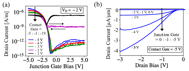
Interestingly, the n-type branch exhibits a much stronger current modulation by the contact gate. In particular, when the contact gate is biased at a negative voltage of \(-5\) V, we observe that the electron current is significantly suppressed, and the device displays only a p-type character with negligible ambipolar behaviour. However, as the bias of the contact gate is made less negative, the current in the n-type branch progressively increases, and eventually, the device exhibits ambipolar characteristics21. This effect is understood by the band diagram in the bottom panel of Figure 1.3. The contact gate primarily controls the electron injection into WSe\(_2\) channel by modulating the thermionic field emission barrier at the /Pt Schottky barrier.
The output characteristics in this mode of operation, shown in Figure 1.4(b), are obtained by keeping the contact gate at a fixed bias of \(-5\) V for different junction gate biases and exhibit good current saturation behaviour. In this mode of operation, this device achieves an on-current of about 8 \(\mu\)A, and an on-off ratio in excess of \(10^8\).
The band diagram and transfer characteristics of the n-type MOSFET mode of operation are shown in Figures 1.5 and 1.5(a) respectively. In this mode of operation, is biased at a positive drain bias, while is kept grounded and acts as the source. The contact gate electrode is biased with a positive voltage, while the junction gate bias is swept from \(-5\) V to \(+5\) V. Note that the p-type branch is nearly suppressed. The n-type branch shows only a weak dependence on the contact gate compared with the modulation by the junction gate21,22. As shown in the band diagram in Figure 1.5, the junction gate efficiently modulates the barrier to the electrons injected from the /Pt contact.
The output characteristics of the device shown in Figure 1.6(b) are obtained by keeping the contact gate bias fixed at \(+5\) V while sweeping the drain bias from 0 to \(+3\) V with junction gate bias as a parameter. These MOSFET characteristics also show good current saturation after pinch-off (\(V_{G}-V_{th}<V_{D}\)). In the MOSFET mode, this device achieves an on-current of about 11 \(\mu\)A, and an on-off ratio in excess of \(10^8\).
Comparing both the modes of operations, we observe that the ambipolar characteristics of the / heterojunction can be completely suppressed by appropriately biasing the gates of the triple-gate structure, achieving a purely n-type (governed by the thermionic process) or p-type operation (governed by band-to-band tunnelling process). This is achieved by adjusting the barrier to carrier injection from metal contacts to . The self-aligned structure of the device ensures that the effect of the contact gate and junction gate on the device operation is independent of each other.
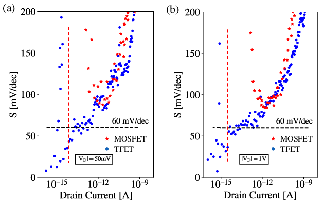
To obtain the subthreshold slope (\(S\)) in the p-TFET (n-MOSFET) mode of operation, we keep the contact gate bias fixed at \(-5\) V (\(+5\) V) and sweep the junction gate bias. The subthreshold slope for both modes of operation, calculated at two different drain voltages (\(|V_{D}|=50\) mV and \(1\) V), is plotted as a function of drain current in Figure 1.7(a-b). The vertical red dashed line indicates the gate leakage current floor. The results clearly indicate the superior subthreshold characteristics for the TFET mode compared with the MOSFET mode. In particular, we reliably extract a minimum subthreshold slope of \(\sim 50\) mV/decade in the TFET mode of operation when the drain current is significantly above the gate leakage floor, while the minimum subthreshold swing in the case of MOSFET is about 75 mV/dec. The leakage floor of the instrument is between \(10^{-14}\) to \(10^{-15}\) A.
In conclusion, we propose and experimentally demonstrate a triple-gated test structure using triple-gated / heterojunction, where a self-alignment is achieved between the source and channel region by exploiting the screening between two partially overlapped gates. As a unique attribute, by tuning the bias at different gate electrodes, the test structure can be independently operated as p-type TFET as well as n-type MOSFET with complete suppression of ambipolar characteristics. With a dual-gated junction control, we obtain excellent subthreshold swing and current saturation from the device, with the minimum subthreshold slope being less than 60 mV/decade in the TFET mode. Such a reconfigurable, multi-functional test structure is interesting for quick performance evaluation of layered-material-based self-aligned field-effect devices without the need for source/drain doping.