Scaling transistors to tiny dimensions has been one of the key reasons behind the onset of the information era. The spread of artificial intelligence and machine learning algorithms on massive data sets has created extreme computing requirements. Such high-performance computing would require transistors that give large current drives with low footprints so that larger systems can be integrated into smaller areas. MBCFETs (Multi-channel bridge FETs) have been promising transistor designs that offer a planar solution to device scaling1. Since 2D transition metal dichalcogenides (TMDs) can be scaled down to a monolayer limit along the vertical dimensions, they are the ideal semiconducting channel materials for MBCFETs. Multibridge channel FET (MBCFET) have been demonstrated in multiple technologies, including Silicon2,3 and 2D materials4–7.
Contact resistance has been one of the key issues in the failure to achieve high-performance 2D transistors8,9. Many solutions have been proposed to mitigate this problem10–14. The most successful solutions to date have been to use novel contact materials, especially semimetals like Bismuth10,14 or Antimony13. In11, a selenium buffer layer has been used to decrease metal-semiconductor interactions and improve contact resistance. In12, . All these methods utilize special contact material or deposition techniques to improve contact resistance. These methods might be, therefore, difficult to integrate into standard process flows.
This chapter proposes a slightly modified 2-channel MBCFET using 2D semiconductors as channel material. We also use graphite, another 2D material, as the contact material. This structure leads to a reduction in the effective contact resistance of the transistor and can be extended to any contact metal if need be. We demonstrate an on-current of 0.43 mA/\(\mathrm{\mu m}\) at a channel length of 1.5 \(\mathrm{\mu m}\) and an on-off ratio of more than \(\mathrm{10^8}\).
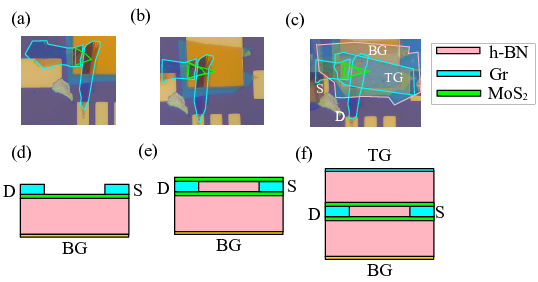
Figure 1.1(f) schematically shows the device structure. Two monolayer channels are stacked on each other, separated by the few-layer graphene contacts acting as source and drain. Two gates are also provided to control both channels. The device is completely symmetric with respect to each channel. Both gates are essential for effective electrostatic control of the channels. These gates have been labelled TG (Top Gate) and BG (Bottom Gate) in Figure 1.1(f). However, owing to the symmetric structure of the device, both gates are equivalent.
The device fabrication is shown schematically in Figure 1.1(d-f). The corresponding optical micrographs are shown in Figure 1.1(a-c). Ti/Au (20 nm/40 nm) contacts are initially patterned on a Silicon substrate with 280 nm \(\mathrm{SiO_2}\) deposited using optical lithography and DC sputtering. A 10 - 15 nm thick h-BN is then dry transferred on the gate contact.15.
This is followed by dry transfer of a monolayer \(\mathrm{MoS_2}\) and the two graphite layers (10 - 15 nm), which act as source and drain. As described in the previous section, Graphite can provide ultra-thin contacts (down to monolayer) while maintaining good stability, which is crucial for device scaling. 1.1 (a) and (d) show the device in this state. The channel length is kept as small as possible, about 1.5 \(\mathrm{\mu}\)m. The device is annealed at this stage in a high vacuum at \(\mathrm{200^oC}\) for three hours. Next (shown in Figure 1.1(b) and (e)), another monolayer is transferred on top of this stack, closely aligning with the previous monolayer. Finally, the top h-BN and the top gate are transferred (acting as the top-gate stack) to complete the device. The device is again annealed in a high vacuum at for three hours. The final device is shown in Figures 1.1(c) and (f).
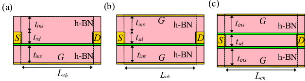
Its scalability is the major advantage of a 2D material-based over a 3D material-based (like Silicon) transistor. Hence, it is important to analyze the short-channel performance of the proposed device structure to be sure that we are not sacrificing the key advantage of the 2D material used for the channel. To analyze the scalability of our proposed design, we simulate three device structures shown in Figure 1.2. Figure 1.2(a) shows the cross-section of a single gate device with a monolayer semiconductor as the semiconducting channel. This structure has only a bottom gate. The simulation details are given in Appendix [transistor-sim]. Although the top side of the channel is covered with an insulator, the whole interface is assumed to be electrostatically open. Figure 1.2b shows the cross-section of a double-gated device with a single monolayer semiconducting channel. In this structure, the top interface is tied to the gate potential. Figure 1.2c shows the proposed device structure. This structure has two monolayer semiconducting channels. Both top and bottom interfaces are gated. The simulation was performed by solving the 2D Poisson equation self-consistently with the drift-diffusion equation.16. We do not consider any source/drain underlap region in all three structures, as underlap regions may contribute to series resistances and increase the device footprint. Each of the structures is characterized by three parameters - \(t_{ins}\), the thickness of the insulator, \(t_{sd}\), the thickness of source and drain contacts and \(L_{ch}\), the channel length.
These parameters are schematically shown for each structure in Figure 1.2. The source/drain thickness \(t_{sd}\) is an essential parameter for 2D transistors, as the short channel effects are influenced by the fringing fields arising from the source/drain contacts17. We select small \(t_{sd}=2\) nm to keep the short channel effects from such fringing fields at a minimum. The requirement for such a small thickness of the source/drain contacts can be fulfilled by using 2D conductors like graphite. The insulator thickness \(t_{ins}\) is taken to be 2 nm. The relative dielectric permittivity of the insulator is assumed to be \(\kappa = 5\). As it has been previously shown17,18, in the case of monolayer 2D semiconducting channels, \(\kappa\) does not play a very significant role in device scaling, and only \(t_{ins}\) does.
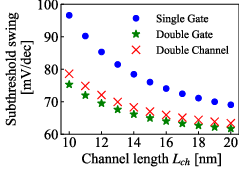
The subthreshold swing as a function of the channel length \(L_{ch}\) is shown in Figure 1.3. \(L_{ch}\) varies from 10 nm to 20 nm. As expected, the single gate device shows a higher subthreshold swing (shown in blue dots) due to poor gate electrostatic control. However, the subthreshold swing of the double gated single channel device (shown in green stars) and the double-channel device (shown in red crosses) is nearly the same. The double-gated device exhibits slightly better subthreshold swing compared to the dual-channel device. Although in the dual-channel device, there is only one gate per channel, compared to two gates per channel in a double-gate device, the stacking of the two monolayer channels on top of each other improves the electrostatics of the device. However, in the case of the single-gated device structure, the top side of the channel is electrostatically open, degrading the device’s performance.
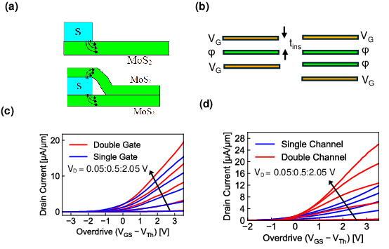
Gate capacitance is also an important factor along with the on-current for overall circuit speed. A higher gate capacitance would, in general, mean a slower speed. The gate capacitance of a single channel device in the on condition with a single gate is given by \(C_{0} = WL\epsilon_{ins}/t_{ins}\), where \(L\) is the channel length and \(t_{ins}\) is the thickness of the gate dielectric with a dielectric constant \(\epsilon_{ins}\). As shown in Figure 1.4(b), the proposed device structure is equivalent to two single-channel devices and a gate capacitance \(C_{DC}=2C_0\). Similarly, a double-gate transistor also has a gate capacitance \(C_{DG}=2C_0\).
The current injection mechanisms of single-channel and double-channel devices are shown in Figure 1.4(a), top and bottom panels, respectively. Since we use a very low resistance contact like graphite, the current injection is not limited by the contact itself but by the interface between the contact and the semiconductor. Therefore, providing two channels to the contact will improve the contact resistance by approximately a factor of two.
Comparison with single gate device: Regarding on-current and gate capacitance, our proposed device structure is equivalent to a single gate device with twice the channel width \(2W\). However, as the previous section shows, a single-gate device performs poorly at shorter channel lengths. Therefore, placing the channel vertically, as in our proposed structure, improves the drain current and the electrostatic integrity.
Comparison with double gate device: A double-gate device should ideally give the same drain current for a similar gate overdrive voltage since the current in a transistor is given by
\[I_D = \frac{\mu C_{ins}W}{L}(V_{GS}-V_T)^2\]
However, this is not the case practically since the current situation is limited by contact resistance. This is shown in Figure 1.4(c). The figure shows the transfer characteristics of a single-channel device with a single gate and double gates. As can be seen, although the drain current improves slightly, it does not double as expected. This is because the current is limited by contact resistance. However, as shown in Figure 1.4(d), the current nearly doubles for the proposed double-channel device, with the same gate capacitance as that of the double-gate structure compared to a single-channel single-gated device.
Therefore, the proposed double channel effectively reduces the contact resistance without increasing the device footprint and gate capacitance, maintaining good electrostatic integrity.
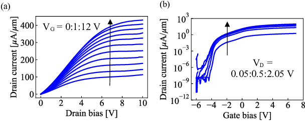
Next, the device’s characteristics are shown with two semiconducting channels in Figures 1.5(a-b). Figure 1.5(a) shows the output characteristics of the device. As can be seen, the device offers an on-current of about 430 \(\mathrm{\mu A}\)/\(\mathrm{\mu A}\) at a drain bias of 10 V and a gate bias of 12 V. Due to a larger channel length, a higher drain bias is applied to provide a sufficient electric field. Channel length scaling to lower dimensions may ease this requirement. We also note that the device current is somewhat restricted by the contact resistance of the Graphite-\(\mathrm{MoS_2}\) interface. This phenomenon can be observed at the high gate and drain bias, where the characteristics start crowding together and no longer increase with linear or square dependence, as the conventional MOSFET theory suggests. The transfer characteristics of the device are shown . The device offers an on-off ratio of more than \(\mathrm{10^8}\). The subthreshold slope of the device at a drain bias of 1 V is about 120 mV/dec. Characterization of another device is given in Appendix [another-transistor-char].
In conclusion, we have analyzed and demonstrated a double channel device design that exhibits an on-current of about 430 \(\mathrm{\mu A/ \mu m}\) with a good on-off ratio and subthreshold swing. The fabrication process of the device is simple, and the device design is scalable to lower channel lengths, improving the effective contact resistance of the device.