Infrared (IR) photodetection is of great importance for a wide variety of technologies. Photodetection in the wavelength range in the C band (1528–1561 nm) and the L band (1561–1620 nm) is of great interest for optical communication systems1,2. IR photodetectors also find extensive applications in imaging3, spectroscopy4, night vision cameras5, and non-invasive biomedical applications6. Conventional inter-band photodetectors, where incident photons excite valence band electrons to the conduction band, are limited by their bandgap to detect long wavelength (lower energy) IR radiation. Thus, one must use narrow bandgap semiconductors to detect infrared photons. Unfortunately, these low-bandgap materials usually suffer from problems with stability, complex growth techniques, challenges in integration into standard fabrication flows, and often possess environment-safety-and-health (ESH) related concerns7–9.
To this end, two-dimensional layered materials have garnered significant attention in the last decade owing to their extraordinary electrical, mechanical and optical properties10–15. Gate-tunability and ease of formation of atomically smooth heterojunctions, with a large library of materials, made them highly attractive for sensitive photodetection applications16,17, including the IR regime18–24. Unfortunately, there are similar concerns, as stated above, regarding the narrow bandgap layered materials as well23,25.
Using widely available, air-stable, wide bandgap materials for IR detection alleviates most of the above problems. However, the use of such materials would require a fundamentally different photodetection mechanism. A well-known mechanism is the intraband photo-excitation of carriers and subsequent collection of the hot carriers through a heterojunction26,27, also called internal photoemission. Schottky diodes26,28–30, and more recently Graphene / 3D semiconductor Schottky junctions31–34 and metal/2D Semiconductor Schottky junctions35–38 have been widely explored for this purpose.
Unfortunately, due to the reasons stated below, for these Schottky junctions, and more so for those which use 2D layered materials, the achieved internal quantum efficiency is poor, plaguing the achievable photodetection efficiency and hence limiting their widespread applications. This work aims to propose and demonstrate a different class of intraband IR detector that intrinsically addresses this issue.
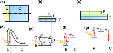
A typical Schottky photodiode utilizes the heterojunction between a metal and a bulk semiconductor as shown in Figure 1.1a. When the metal absorbs photons with energy above the Schottky barrier height (SBH), the hot carriers overcome the barrier and get injected into the semiconductor39,40. The built-in electric field in the semiconductor due to band bending pulls the hot carriers away from the junction (Figure 1.1d). The primary bottleneck in the internal quantum efficiency arises from the large free electron density in the metal, which causes rapid carrier relaxation due to ultrafast electron-electron (e-e) scattering. This results in a small fraction of the generated hot electrons to overcome the Schottky barrier.
When an ultra-thin layered semiconductor replaces the bulk semiconductor (Figure 1.1b), and the photocarriers are extracted laterally, there is an additional mechanism that further plagues the quantum efficiency of the photodetector, as explained using the band diagrams in Figure 1.1e-f. These two band diagrams are plotted along the lateral dashed black line and vertical dashed magenta line in Figure 1.1b. Note that the electric field exponentially drops in the lateral direction within a transfer length (\(L_T\)) from the metal-semiconductor contact edge41–43, as marked by the dashed box in Figures 1.1b-e - degrading the drift of the photo-generated electrons under the metal-semiconductor overlap area. On the other hand, being the energetically favourable process, the photo-induced carriers injected from metal to the layered material are transferred back to the metal at a fast timescale (\(\tau_{sm}\)) (see Figure 1.1f). \(\tau_{sm}\) is far shorter than the time (\(\tau_l\)) it takes for the carrier to traverse the lateral metal-semiconductor overlap area. This results in poor carrier injection efficiency unless the photocarrier is generated adjacent to the metal-semiconductor edge36,41. This effectively reduces the active area of the photodetector, eventually resulting in a weak photoresponse.
To circumvent these problems, we propose to use an asymmetric double heterostructure with a thin barrier layer being sandwiched between the emitter (carrier injector) and the collector layers (Figure 1.1c). Unlike a typical Schottky barrier diode, the collector conduction band (CB) edge is chosen to be energetically lower than the emitter, as shown in Figure 1.1g. The proposed structure has several important features: (a) The light absorption occurs in a doped semiconductor instead of a metal, and we show later that the interplay between the availability of free electrons and e-e scattering dictates an optimum doping that provides the maximum photoresponse. A gate voltage tunes the doping in the absorbing layer. (b) The band-offsets of the constituting layers are chosen so that the heterojunction acts as a valve. Once the hot electrons are transferred from the emitter layer to the collector layer and relax to the band edge, the back transfer probability is minimal due to the high energy cost. We note that fast carrier relaxation is detrimental in the emitter but is desirable in the collector as it reduces back transfer probability. Thus, choosing a metal as the collector layer further helps to improve the photoresponse. (c) The asymmetric band-offsets also help towards the unidirectional flow of photocurrent, improving the overall efficiency (indicated by the thickness of arrows in Figure 1.2). (d) The metal also acts as a back reflector for the incident photons, and the thickness of the entire stack is optimized to improve absorption.
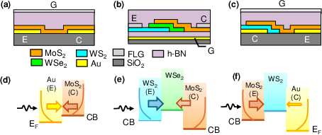
We perform a systematic study by fabricating three structures (D1, D2, and D3), as schematically depicted in Figures 1.2a-c. Figures 1.2d-f show the corresponding band diagrams. The thickness of the different layered semiconductors (, , and ) used is \(\sim\)5 nm in all the devices. All the devices are encapsulated using h-BN to provide stability from ambient conditions. Further, the devices are annealed at 150 \(\mathrm{^oC}\) in a vacuum for three hours to provide good contact between the layers. In D1, we directly place on Au film, making a conventional Schottky photodiode. D2 consists of a stack of // layers. The infrared photons excite electrons in the conduction band of the emitter layer, which are collected by the collector through the barrier layer. However, the electrons excited in the collector layer find it difficult to cross the barrier due to the larger barrier to . Finally, in D3, a barrier layer is sandwiched between Au collector and emitter layers. As shown in Figures 1.2a-c, all three structures are controlled by a gate voltage (\(V_G\)).
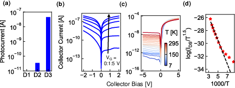
Figure 1.3a shows the relative photoresponse of the three structures when excited with the same optical power (\(P_{op}\)) of 1550 nm radiation. D1 shows no measurable photocurrent (\(I_{ph}\))36, likely due to strong backscattering, as discussed above. D2 and D3 exhibit appreciable photoresponse; however, \(I_{ph}\) from D3 is about 1000-fold stronger than that of D2. The enhanced structural asymmetry and fast relaxation of the injected carriers in the Au collector layer improve the unidirectional flow of \(I_{ph}\) in D3 (Figures 1.2e-f).
To understand the difference in asymmetry between D2 and D3, we perform current-voltage characteristics in the dark condition (Figure 1.3b-c). The results suggest a more diode-like behaviour in D3 compared with D2, which results in stronger asymmetry. Further, we show the current-voltage characteristics for D3 at different temperatures (Figure 1.3b). Note that when the electrons are injected from Au to (negative collector bias), there is a strong temperature dependence, indicating thermionic emission. We extract an effective SBH of about 0.16 eV from the temperature dependence, as shown in Figure 1.3d. On the other hand, when electrons are injected from to Au (positive collector bias), the temperature dependence is negligible, suggesting that the carriers tunnel through the barrier layer.
When illuminated, the electrons in the conduction band of the emitter layer are excited to higher energy states. These non-equilibrium high energy electrons (hot electrons), in turn, relax initially through e-e scattering in an ultrafast time scale (\(\tau_{ee}\)) and eventually through phonon scattering at a relatively longer timescale (\(\tau_{p}\))44–46. However, in the van der Waals junctions under consideration, the hot electrons are also transferred from the emitter to the collector at a fast timescale (\(\tau_{ec}\)), with \(\tau_{ee} < \tau_{ec} < \tau_{p}\). Thus, essentially, the injection efficiency to the collector is controlled by the e-e scattering rate, which, in turn, can be controlled by tuning the free electron density in the emitter layer through a gate voltage (\(V_G\)).
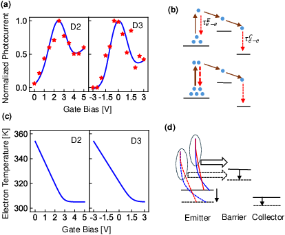
We plot the \(V_G\) dependence of \(I_{ph}\) for both D2 and D3 in the left and right panels of Figure 1.4a, respectively. For both the devices, \(I_{ph}\) initially increases with an increase in \(V_G\), reaching a maximum value, followed by a reduction in \(I_{ph}\) with a further increase in \(V_G\). At large \(V_G\), we again observe a weak increasing trend of \(I_{ph}\) with \(V_G\). The initial increase in \(I_{ph}\) is expected due to an increase in the available number of electrons that can be excited to higher energy states by the incoming infrared radiation (see top panel of Figure 1.4b). However, when the electron density increases significantly (bottom panel of Figure 1.4b), the fast relaxation due to enhanced e-e scattering tends to quench the hot electron density, reducing the injection efficiency to the collector, thus degrading the net \(I_{ph}\).
We develop a simple physical model to explain such nonmonotonic behaviour quantitatively, as schematically explained in the bottom panel of Figure 1.4d. The details of the model are described in Appendix [hot-electron-model]. We solve the Poisson equation along the vertical dimension to obtain the electrostatic potential of each layer under dark conditions. We assume that, under illumination, the nonequilibrium electrons available for transfer to the collector can be described by Fermi-Dirac statistics with a higher electron temperature (\(T_e\)) compared to the lattice temperature (\(T_L\)). \(T_e\) is primarily governed by the e-e scattering under the condition of \(\tau_{ee} < \tau_{ec} < \tau_{p}\). A higher \(T_e\) broadens the electron distribution with a longer high energy tail, thus allowing more electrons to cross the barrier layer (Figure 1.4d). We use \(T_e\) as a fitting parameter. The model predicted \(I_{ph}\) is shown in blue traces in Figure 1.4a, and the corresponding fitted \(T_e\) is depicted as a function of \(V_G\) in Figure 1.4c.
Consider the case of small \(V_G\) in Figure 1.4d. The conduction band edges are shown in black solid lines, and the corresponding electron distributions with and without photoexcitation are shown in blue and red continuous traces, respectively. Both are calculated, keeping the total electron concentration in the conduction band fixed. This is achieved by calculating a new quasi-Fermi level under illumination. The broader electron distribution under illumination allows more carriers to cross the barrier.
At higher \(V_G\), the free electron density increases under dark conditions, and the band edges are energetically shifted downward (shown in black dashed lines). This increment in the available free electron density results in an enhanced \(I_{ph}\) (the rising part in Figure 1.4a). However, with further increase in \(V_G\), \(T_e\) also decreases due to faster e-e scattering (Figure 1.4d), resulting in a narrower electron distribution (dashed traces in blue and red under dark and illumination conditions, respectively), eventually reducing \(I_{ph}\). Figure 1.4c indicates that the fitted \(T_e\) gradually reduces with \(V_G\) for both D2 and D3, as expected. With an even further increase in \(V_G\), the increase in electron concentration slows down significantly due to screening, which in turn flattens out \(T_e\) and results in either flattening or slight increment in \(I_{ph}\) again. The results suggest an intricate way to tune the quantum efficiency of the photodetector by controlling e-e scattering.
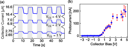
We now focus on device D3 for analyzing the IR detection performance. To understand the steady-state \(I_{ph}\) characteristics under 1550 nm excitation, we plot in Figure 1.5a the device current of D3 under laser on (shaded regions) and off conditions at various collector bias (\(V_{CE}\)) values. The magnitude of the device current systematically increases with \(V_{CE}\). The corresponding photocurrent (\(I_{ph} = I_{light}-I_{dark}\)) is plotted in Figure 1.5b. Due to an increased bias, a higher electric field helps the electrons excited in the emitter layer to quickly escape to the collector before relaxation, increasing \(I_{ph}\). However, due to an increase in \(I_{dark}\), larger \(V_{CE}\) also increases the shot noise, as clearly observed in Figure 1.5b.
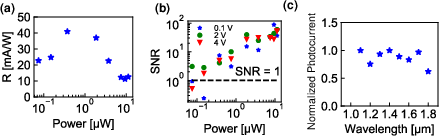
The corresponding responsivity (\(R={I_{ph}}/{P_{op}}\) at \(V_{CE}=4\) V) is plotted in Figure 1.6a as a function of incident optical power (\(P_{op}\)), showing a maximum \(R\) of 42 mA/W. Note that, unlike typical 2D material-based photodetectors, \(R\) remains a weak function of \(P_{op}\) in the entire range, suggesting a negligible role of photocarrier recombination and trapping effects.
We extract the noise amplitude (\(N\)) from the low-frequency temporal response of D3 (Figure 1.5a) by calculating the standard deviation of the device current under optical illumination. The corresponding signal-to-noise ratio (\(\mathrm{SNR} = \frac{I_{ph}}{N}\)) is plotted in Figure 1.6b as a function of \(P_{op}\), for different \(V_{CE}\). Interestingly, at low \(P_{op}\), we obtain higher SNR at \(V_{CE}=2\) V compared with \(V_{CE}=4\) V due to enhanced shot noise at higher bias. This suggests that an optimal \(V_{CE}\) exists for weak signal detection to maximize SNR.
The photoresponse of D3 is nearly flat from 1100 nm to 1800 nm excitation (Figure 1.6c). A similar broad response is obtained from D2 as well (see Appendix [wav-response-of-d2]). This broad response arises because the photon energy at this wavelength range is significantly higher than the band offset between the emitter and the barrier layer. The results from another fabrication run of D3 are shown in Appendix [char-of-d3-device].
Next, we measure the frequency response of D3 using a setup shown in Figure 1.7a. The detector is connected to a \(V_{BIAS}=-4\) V through an external load resistor (\(R_L\)) of 570 \(k\Omega\), which helps convert the output current to a voltage signal. The signal from the photodetector is fed to a JFET-based single-stage amplifier with a load resistance (\(R_D\)) of 100 \(\Omega\). The JFET is biased with a \(V_{DD}=3\) V. The detector, external resistors and the JFET are integrated into a printed circuit board (PCB) (onset in Figure 1.7a). The signal output is then further bandpass-filtered with an input gain of 20 dB and observed in an oscilloscope.
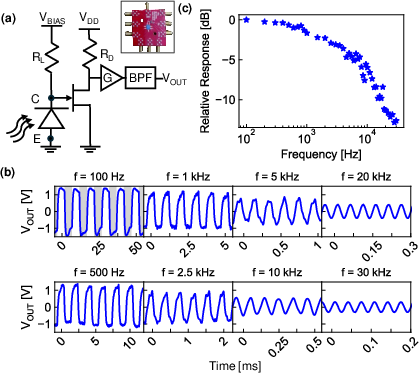
The photodetector is illuminated with a 1550 nm laser at varying frequencies. The temporal response of the signal for different frequencies is shown in Figure 1.7b. The time during which light is illuminated is shown in grey bands in the top left panel. The signal output progressively diminishes with higher frequencies. A signal above the noise floor could be observed up to \(\sim\)30 KHz. Figure 1.7c shows relative photoresponse (in dB) as a function of the laser intensity modulation frequency.
The measured frequency response is primarily limited by the gain-bandwidth product of the external measurement setup and not by the intrinsic device. The limiting factor likely arises from the relatively large input capacitance of the JFET. The intrinsic response from the device itself could be much faster, as all the physical processes involved in the detection mechanism are fast. In Appendix [freq-red-laser], we show the device’s response to 633 nm excitation (which allows bandgap absorption and hence a stronger signal), demonstrating a detectable response above the noise floor up to 100 KHz.
To conclude, we demonstrate a different class of intra-band photodetector with intrinsically improved internal quantum efficiency through elegant hot electron management. The simplicity of the design makes the device readily integrable with different photo-excitation schemes, such as with a waveguide. We also demonstrate the heterogeneous integration of the photodetector chip with post-processing electronics on a printed circuit board, making it immediately usable at a system level.