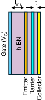
The structure used in the physical model for the device is shown in the figure below. The emitter, barrier and collector layers are considered thin, separated by a physical distance \(t\).This distance is typically the van-der Waal gap between the material.
Since the layers are assumed thin, they are each equipotential, with the electrostatic potential of the three layers denoted by \(\phi_{E}\), \(\phi_{B}\) and \(\phi_{C}\). The system of equations that govern the system are -
\[\begin{aligned} \epsilon \frac{\phi_{E} - V_G}{t_{ins}} + \epsilon \frac{\phi_{E} - \phi_{B}}{t} &= e(N_{DE} - n_{E})\\ \epsilon \frac{\phi_{B} - \phi_{E}}{t} + \epsilon \frac{\phi_{B} - \phi_{C}}{t} &= e(N_{DB} - n_{B})\\ \epsilon \frac{\phi_{C} - \phi_{B}}{t} &= e(N_{DC} - n_{C})\ \end{aligned}\]
where \(N_D\) and \(n\) represent the fixed doping concentration and electron concentration inside the respective layer, while \(e\) is the absolute charge of an electron. The carrier concentration is related to the electrostatic potential of the layer by -
\[\begin{aligned} n(\phi, T, E_F) = \frac{g_sg_vm^*k_BT}{\pi\hbar^2}\log\Big(1+\exp\Big(\frac{e(E_F-D+\phi)}{k_BT}\Big)\Big) \end{aligned}\]
where \(g_s\) and \(g_v\) are spin and valley degeneracies, respectively. \(E_F\) is the fermi level. Under dark conditions, \(E_F=0\). \(D\) is the position of the conduction band with respect to Fermi level \(E_F=0\) at \(\phi=0\). This parameter represents the doping of the layer.
Under illumination, we assume the temperature of the electrons to be \(T_e > T\) in both collector and emitter layers. Unlike an inter-band photoexcitation, the number of carriers in the conduction band will remain constant. Also, since the carrier concentration does not change, we do not expect the electrostatic potentials to change either. Using these constraints, we can calculate the new quasi-Fermi level, \(E_{Fe}\) using -
\[\begin{aligned} n(\phi, T, E_F=0) = n(\phi, T_e, E_{Fe}) \end{aligned}\]
The new quasi-Fermi level and the higher temperature define the distribution of electrons in the conduction band under illumination.
Once the distribution is obtained, the number of carriers in the emitter layer with energy higher than the conduction band edge of the barrier layer is calculated (\(n_{E}(T^{E}_{e})\)). Similarly, the number of carriers in the layer with energy greater than the barrier layer conduction band edge is calculated ((\(n_{C}(T^{C}_{e})\))). The photocurrent, then, is proportional to the difference between the two.
\[I_{ph} \propto n_{E}(T^{E}_{e}) - n_{C}(T^{C}_{e})\]
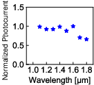
D2 exhibits a similar wavelength response to various radiation of the SWIR spectrum as D3.
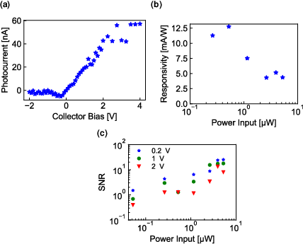
The results of the characterization of device D3 from another fabrication run are shown in the figure below. The device shows qualitatively similar behaviour as the device presented in the main text. The device shows a peak responsivity of 12.5 mA/W.
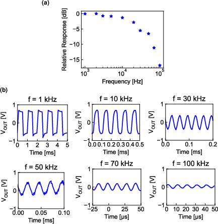
With 633 nm radiation, we can detect signals up to 100 kHz with the same device.