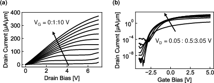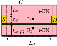
A typical double-gate monolayer 2D material-based transistor is shown in the figure below.
The channel is considered infinitely thin. In the insulating regions, electrostatic potential is obtained by solving the Laplace equation.
\[\frac{\partial^2\phi}{\partial x^2} + \frac{\partial^2\phi}{\partial x^2} = 0\]
Along the semiconductor channel, electrostatic potential is obtained by satisfying the discontinuity condition of the displacement vector by surface charge density.
\[\epsilon_{ins}(E_1 + E_2) = q(N_D - n + p)\]
where \(E_1\) and \(E_2\) are electric fields, as shown in the figure above. \(N_D\), \(n\) and \(p\) are surface dopant, electron and hole concentrations, respectively, and \(q\) is the fundamental electron concentration. For \(n\)-type wide bandgap material like \(\mathrm{MoS_2}\), the hole concentration \(p\) can be neglected. These equations are solved using a finite differences numerical scheme.
The electron concentration \(n\) is obtained by solving the current (\(J_e\)) continuity equation in the channel.
\[\vec{\nabla}\cdot \vec{J}_e = 0\]
When coupled with drift-diffusion transport, the continuity equation is solved efficiently using the Gummel-Scharfetter numerical scheme. The continuity equation is then solved self-consistently with the Laplace equation to obtain electrostatic potential and the charge concentration in the device.
Boundary conditions At open boundaries, the electric field normal to the surface is considered zero (Neumann boundary condition). At the terminals (source, drain and gate), the electrostatic potential is assigned the value of the given terminal potential (Dirichlet boundary condition). Similarly, at the boundaries (i.e. at the contacts), the electron concentration in the channel is assigned the equilibrium electron concentration (inherently, this assumes an infinite recombination velocity at the contacts).