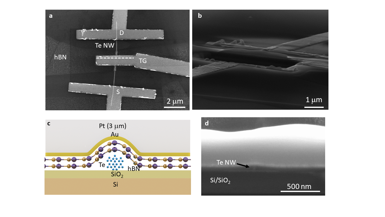
The Te nanowires are synthesized using \(\mathrm{Na_{2}TeO_{3}}\) as a precursor in the water medium, where hydrazine hydrate is used as a reducing agent, Polyvinylpyrrolidone( PVP) as a capping agent, and Ammonia is used to maintain proper pH. In a typical experiment, 1 g of PVP (average. M.W.= 58,000) is dissolved in 20 ml of DI water and 92 mg \(\mathrm{Na_{2}TeO_{3}}\) is dissolved in 15 ml DI water separately. Both solutions are mixed at room temperature. Into the above solution, 1.5 ml of Hydrazine hydrate and 3.3 ml of 25% aqueous ammonia solution are added drop-wise with moderate stirring. The transparent solution is then transferred to a 50 ml capacity teflon container. Then the hydrothermal reaction is allowed to take place for 4 hours at \(180\mathrm{^{\circ}C}\). After the reaction vessel cools down to room temperature, the solution is cleaned twelve times using hot water (\(60^{\mathrm{\circ}}\mathrm{C}\)) at 8000 revolutions per minute and subsequently two times using ethanol.
X-ray diffraction measurement has been carried out using Rigaku X-ray Diffractometer with Cu \(\mathrm{K\alpha}\) source. Microstructural characterization has been done using FEI Tecnai T20 S-Twin (200 kV) and FEI-Titan G2 60-300 microscope operated at 300 kV. To get a cross-sectional view of the device, the desired pattern has been made using FEI Helios G4 UX FIB instrument with Ga ion beam source operated at 30 kV (current \(\sim 1.6\) nA) after depositing the device with Pt (\(\sim 3\) micron thick).
The solution synthesized nanowires were first drop cast on \(\mathrm{p^{++}}\) Si substrate with 285 nm \(\mathrm{SiO_{2}}\) grown on top. The substrate is the Argon plasma cleaned at a power of 10 W and a pressure of 10 mbar for 20 s in PlasmaLab system 100 ICP 380 from Oxford instruments. A thin layer of hBN is then transferred using a dry transfer method. The substrate is then spin-coated with PMMA C3 and baked on a hot plate at \(180^\circ\) C for 2 minutes. e-Beam lithography is then performed to define the source, drain, and gate contacts. Patterns are then developed in MIBK:IPA solution in 1:3 ratio. Substrate is then immediately plasma cleaned once again using the same parameters. Ni/Au (20 nm/40 nm) is then deposited on the substrate using DC magnetron sputtering. Finally, lift-off is performed by dipping the substrate in acetone for 10 minutes, followed by drying.
Room temperature device characterization was done in ambient conditions using a B1500 semiconductor parameter analyzer. Low-temperature characterization was performed by loading the substrate in Montana cryostation using a Keithley 4200A semiconductor parameter analyzer.
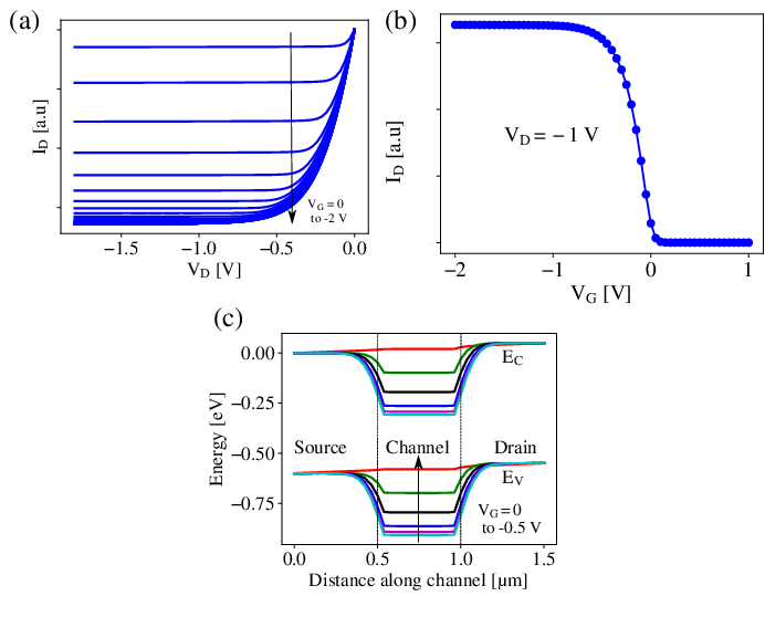
To gain a deeper understanding of the operation of the junctionless transistors, drift-diffusion simulations were performed (as described in Appendix [transistor-sim], assuming a charge sheet model and solving Shockley equations consistently. Band gap of the material is assumed 0.6 eV, default doping is defined by \(E_F - E_V = 0.2\) eV.